Edge AI PCB Assembly: A Prototype-to-Low-Volume Manufacturing Checklist
A manufacturing-readiness guide for edge AI hardware teams planning BOM sourcing, BGA assembly, power and thermal validation, programming, testing, and repeatable low-volume builds.
Engineering review by Huitai Engineering Team
Quick Answer
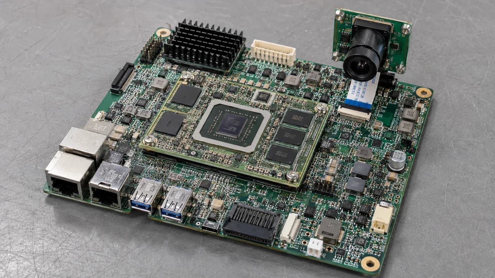
Edge AI PCB assembly often places more manufacturing pressure on a board than a basic IoT design because the processor, memory, storage, high-speed interfaces, and power rails must work together under changing compute loads. Before requesting a prototype or low-volume production quote, prepare the fabrication files, BOM, component placement data, assembly drawings, PCB specifications, firmware and programming method, and a functional testing procedure with measurable pass/fail criteria. A complete package lets the manufacturer review what can be built, purchased, assembled, programmed, and tested without guessing.
Power delivery and thermal preparation deserve early attention because an accelerator or processor may draw short current peaks and generate concentrated heat. Fine-pitch BGA packages may require tighter process controls and, depending on the design, X-ray inspection. LPDDR, eMMC, NVMe storage, PMICs, camera modules, and specialized connectors may also create lifecycle or lead-time risk. The goal is not to specify every advanced process by default. It is to identify the risks that apply to this board, document customer-controlled decisions, and establish a repeatable path from engineering samples to stable batches.
In this guide: development path, BOM risk, PCB and BGA requirements, power and thermal preparation, testing, and the RFQ checklist.
What Makes an Edge AI PCBA Different?
An edge AI board processes data locally, often close to a camera, sensor, machine, or gateway. That does not automatically make every design difficult to manufacture, but it may combine dense computing, memory, power conversion, and fast interfaces in less space than an ordinary connected sensor node. The table below describes common differences, not universal rules.
| Area | Ordinary IoT PCB | Edge AI PCB |
|---|---|---|
| Processor | Often a microcontroller or modest application processor | May use an application processor, AI accelerator, NPU, GPU, or high-performance SoM |
| Power demand | Often low and relatively steady, depending on radio duty cycle and loads | Often higher and more dynamic, with startup and inference-related current changes |
| Memory and storage | May use internal memory plus limited external flash | Often uses external LPDDR and eMMC, and in some projects NVMe storage |
| High-speed interfaces | Commonly UART, SPI, I2C, USB, Ethernet, or wireless | May add MIPI camera links, PCIe, USB 3.x, Gigabit Ethernet, high-speed memory, or display interfaces |
| Thermal requirements | Frequently manageable through normal copper and enclosure design | Often needs deliberate heat spreading, thermal vias, interface materials, heat sinks, or airflow |
| Inspection and testing | AOI and a basic functional sequence may be sufficient | Fine-pitch BGA inspection, programming, interface tests, load behavior, and extended runtime checks may be required |
Manufacturing complexity depends on the actual layout, package types, stackup, materials, interfaces, operating environment, and acceptance plan. A small SoM carrier can be straightforward, while a compact board with directly mounted processing and memory can require more detailed fabrication, assembly, and test preparation.
Development Board, SoM, or Custom PCB?
The hardware architecture determines how much design risk remains when the project reaches a PCBA manufacturer. Teams typically move through one of three paths, and the correct path depends on schedule, volume, size, cost, performance, and the engineering resources available.
1. Development board
A development board is useful for evaluating a processor, software stack, camera, sensor, and early model performance. It shortens the learning cycle but may include unused connectors, oversized power circuitry, or features that do not fit the final product. Treat it as a reference platform, not automatically as production documentation.
2. SoM with a custom carrier board
A system-on-module can keep the processor, memory, and some power functions on a proven module while the carrier provides product-specific connectors, power input, networking, cameras, sensors, and mechanical interfaces. This often reduces routing and BGA integration risk, although module availability, lifecycle, connector choice, and carrier-board testing still need review.
3. Processor integrated directly on a custom PCB
Direct integration can reduce size and recurring module cost or provide tighter control over interfaces. It also moves memory routing, processor power sequencing, BGA escape, signal integrity, boot configuration, and thermal implementation into the customer design. This path often needs the most complete design verification before manufacturing release.
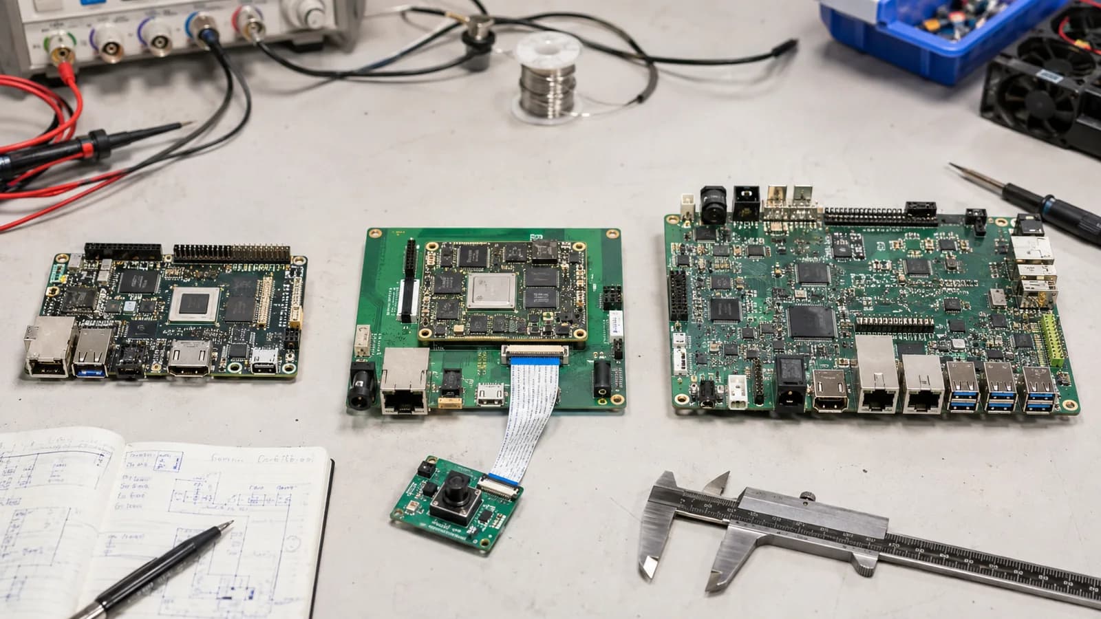
A PCBA manufacturer can review manufacturing files, footprints, component data, assembly constraints, inspection needs, programming inputs, and the agreed test scope. That review can identify missing or conflicting information. It does not replace the customer hardware team, algorithm developers, certification specialists, or product-validation process, and it cannot prove that the system architecture or AI model meets the product requirement.
BOM and Component Sourcing Risks
The BOM is both a purchasing document and a technical control record. Edge AI projects often concentrate risk in a few expensive or single-source items: the AI processor or SoM, PMIC, DC-DC regulators, LPDDR, eMMC or NVMe storage, high-capacitance MLCCs, high-speed connectors, camera and sensor modules, and wireless modules. Check exact manufacturer part numbers, packages, temperature grades, moisture sensitivity where relevant, lifecycle status, authorized supply options, and required quantities before committing the build schedule.
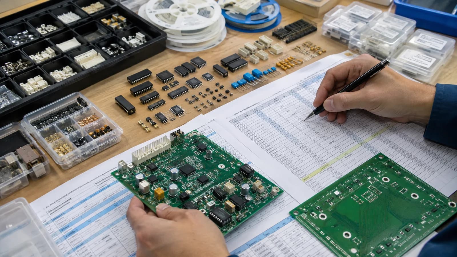
Long-lead and single-source components should be identified during the prototype phase, not after the design is released for repeat production. The 2026 component shortage guide explains why availability must be checked by exact part and date. Use consistent BOM best practices, an approved vendor list (AVL), and a documented sourcing route for critical parts. The BOM sourcing service can be scoped around those controlled inputs.
Critical components must never be silently replaced. Every alternative needs customer approval and should be tied to the controlled BOM revision. An alternative review cannot rely on a similar part name or package description; it should compare footprint, pinout, electrical ratings, timing, power behavior, interfaces, firmware impact, temperature range, qualification needs, lifecycle, and test coverage. The alternative-component guide covers this decision process in more detail.
For an early quote, state which lines are no-substitute, which substitutions are already approved, whether customer-supplied parts will be used, and whether traceability or country-of-origin restrictions apply. That makes purchasing assumptions visible before orders are placed.
PCB Stackup and Assembly Requirements
Start with fabrication data that matches the electrical and mechanical design: layer count, proposed or controlled stackup, board thickness, copper weight, surface finish, dimensions, tolerances, and any impedance requirements. Identify controlled single-ended nets and differential pairs, including the relevant target impedance and reference layers. High-speed memory, PCIe, USB, Ethernet, MIPI, or display links may need tighter stackup coordination than low-speed control signals.
Package and routing choices drive assembly requirements. BGA and fine-pitch devices may affect stencil design, paste deposition, placement accuracy, reflow profiling, pad finish, handling, and inspection. Via-in-pad should identify whether vias are filled and capped. HDI structures, blind or buried vias, and small laser-drilled features must be completely defined in the fabrication notes rather than inferred from Gerber data.
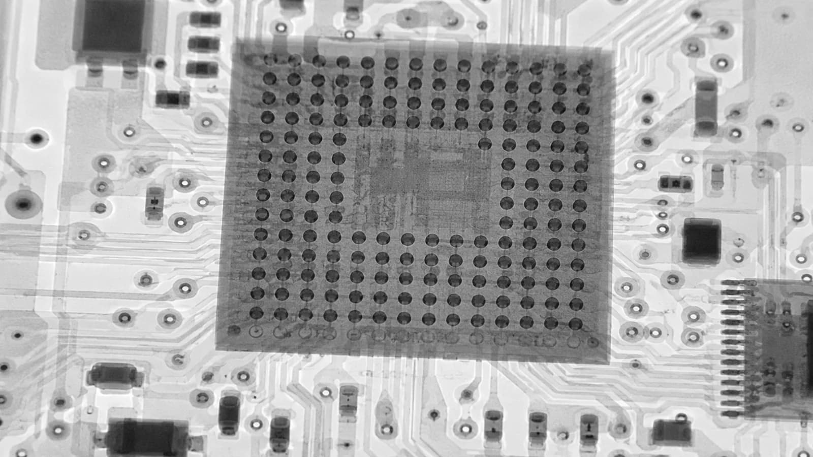
Not every edge AI board requires HDI, advanced materials, or X-ray inspection. These capabilities should be reviewed or coordinated according to package geometry, hidden solder joints, board design, reliability needs, and the agreed inspection plan. A SoM carrier with conventional packages may use a standard multilayer process, while a directly integrated processor and memory design may justify more advanced controls.
Panelization should include practical tooling rails, global and local fiducials where needed, board support, routing or V-score rules, and separation clearance. Confirm component-to-edge spacing, tall-component restrictions, underside clearance, connector overhang, heat-sink access, selective or manual assembly areas, and any mechanical keep-outs. The current capabilities overview is a useful starting point, but the actual stackup, panel, BGA, and inspection scope should be confirmed for the project.
Power Integrity and Thermal Preparation
Edge compute hardware can pass a basic power-on check yet fail during boot, camera startup, networking bursts, or sustained inference. The RFQ and test package should therefore describe both steady operation and meaningful load changes.
Power
Document the input-voltage range, connector polarity, expected steady current, peak current, transient current, and startup current. List the required rails, PMIC or regulator configuration, sequencing dependencies, reset behavior, and any enable or power-good signals. If power modes vary, explain the conditions that trigger each mode and the acceptable voltage limits.
Decoupling selection and placement remain customer design responsibilities, but manufacturing data must correctly identify values, packages, dielectric or voltage ratings where controlled, and do-not-substitute parts. High-capacitance MLCC behavior can change with DC bias, so nominal capacitance alone may not describe the design intent. Provide accessible test points for critical rails, voltage monitoring points, current-limit conditions, and any measurements required during load changes.
Thermal
Identify the main heat sources: processor or accelerator, memory, storage, PMIC, high-current regulators, radios, and interface devices. Define how the product is expected to move heat through copper spreading, thermal vias, thermal pads, a heat spreader or heat sink, enclosure contact, and airflow. Mechanical drawings should show contact surfaces, compression requirements, keep-outs, and the installed enclosure condition when it affects cooling.
Specify ambient-temperature limits, continuous-operation duration, duty cycle, orientation, airflow assumptions, and temperature-monitoring points. If the customer requires thermocouple locations, on-board sensor readings, surface-temperature limits, or an extended runtime sequence, include them in the test procedure. A PCBA review can coordinate build and measurement requirements; product thermal simulation and final system qualification remain with the customer unless separately defined by a qualified provider.
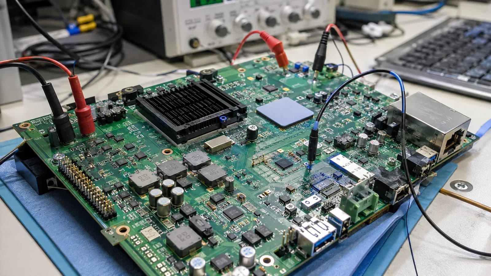
Inspection, Programming, and Functional Testing
A practical quality plan starts with incoming inspection of controlled PCB and component attributes, then applies solder-paste inspection (SPI) where applicable, automated optical inspection (AOI), and X-ray when package geometry or project risk requires it. Each method has limits: AOI sees visible conditions, while X-ray can examine selected hidden joints but does not prove firmware or product function.
Programming should define the approved firmware revision, file format, programming interface, tool or adapter, security or key-handling responsibility, configuration steps, serialization, and the evidence to record. Functional testing then exercises defined board behavior. An AI camera might check power rails, image capture, a network link, and selected I/O. An edge gateway might check boot, Ethernet, USB, storage, and communications. A robotics controller might check communications and controlled I/O, while a smart sensor may check readings, calibration status, wireless communication, and power modes.
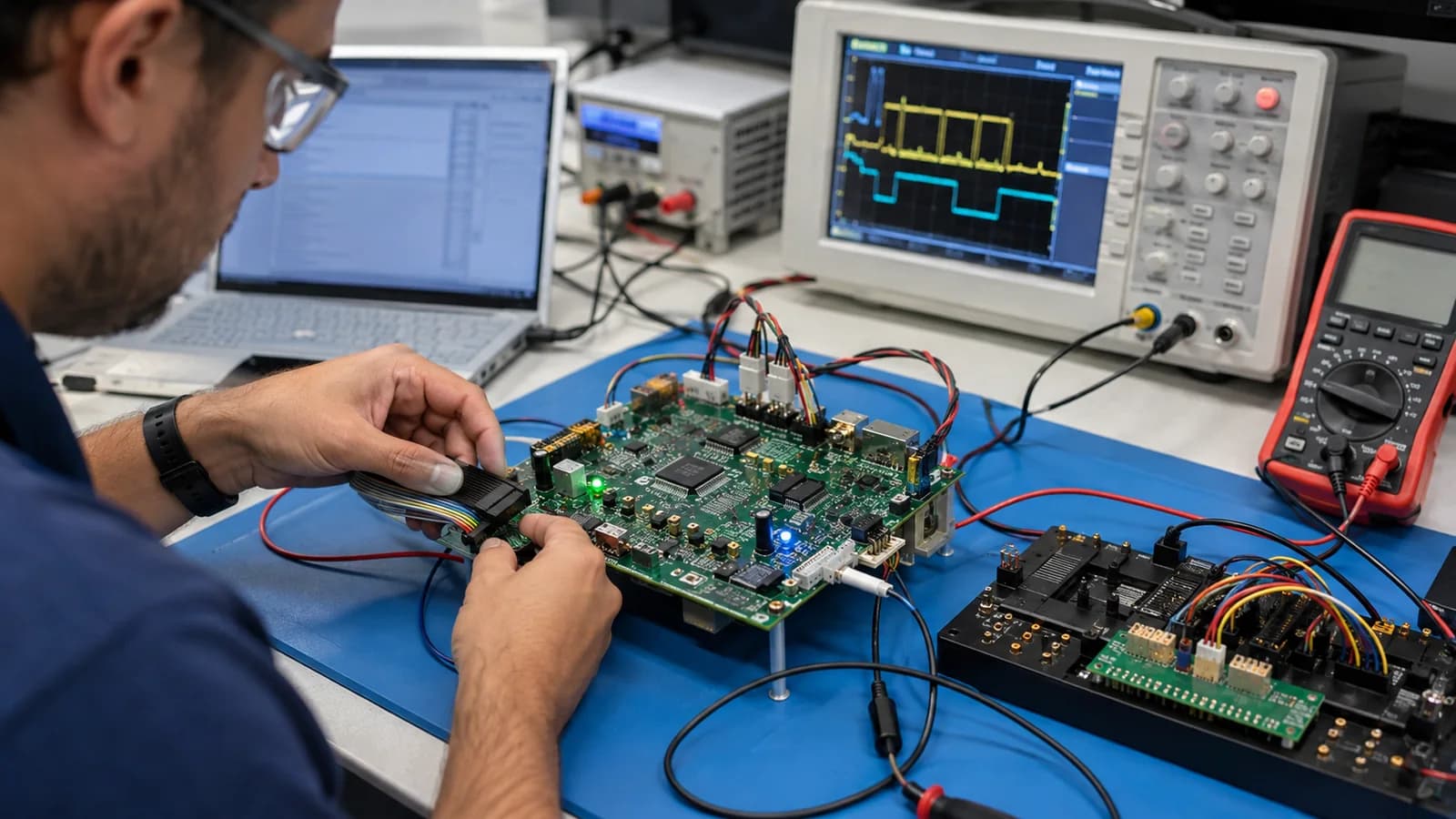
The customer should define the firmware, programming method, fixture, expected outputs, pass/fail criteria, and any model-specific validation requirements. A manufacturer can execute and record an agreed sequence, but should not be assumed to validate AI model accuracy, algorithm quality, dataset coverage, or end-product performance outside that sequence. Use the detailed PCBA testing guide to prepare inputs and align the scope with the testing and quality-control service.
Extended runtime or burn-in can be added when the customer defines duration, load, environment, monitoring, limits, failure handling, and data-retention requirements. It is not an automatic substitute for system qualification, and it should be quoted as a controlled, project-specific operation.
From Five Prototypes to Repeat Production
A typical program may begin with 5-10 prototypes, continue through engineering validation testing (EVT) and design validation testing (DVT), then move to a pilot build, low-volume production, and repeat production. These quantities and stage names are planning examples, not mandatory standards. The right sequence depends on product risk, design maturity, certification, tooling, firmware, supply, and the customer validation plan.
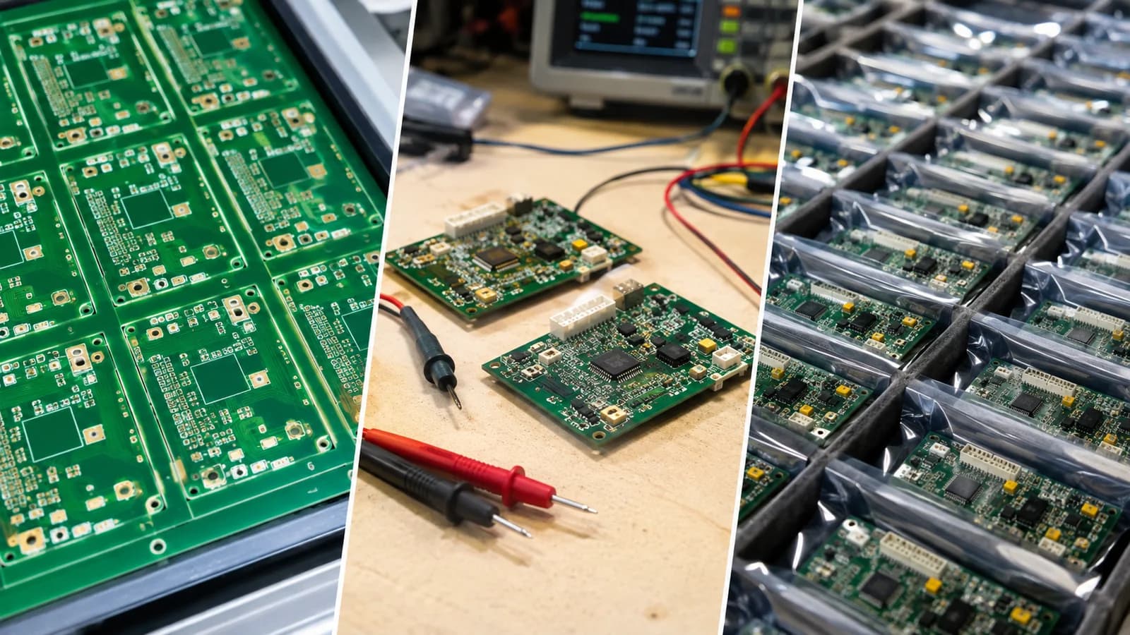
Prototype feedback should become controlled manufacturing data. Correct BOM errors, update footprints or assembly notes, freeze the approved PCB revision, and record firmware versions. A golden sample can help communicate expected assembly and functional behavior, but it should be accompanied by controlled files and measurable acceptance criteria rather than used as the only specification.
Before a pilot or repeat build, prepare the test fixture and programming station, define fixture ownership and maintenance, and verify that the procedure is repeatable. Track first-pass yield and meaningful failure categories so recurring problems can be distinguished from isolated rework. Batch traceability may include PCB revision, BOM revision, firmware, component lots where required, serial numbers, test results, and disposition records.
Approved substitution control is especially important across batches. A part accepted for one revision or validation lot should not automatically carry into another product state without checking the approval conditions. The prototype-versus-low-volume guide explains the transition, while the prototype PCB assembly and low-volume PCBA assembly pages describe the existing service paths.
Edge AI PCBA RFQ Checklist
Use this copyable checklist to make quotation assumptions and customer decisions visible. Mark unavailable items clearly instead of leaving the supplier to infer them.
- Gerber files and drill data for the intended revision
- BOM with exact manufacturer part numbers and reference designators
- CPL / pick-and-place file with side, coordinates, and rotation
- Assembly drawings with polarity and special instructions
- PCB specification covering material, thickness, copper weight, finish, color, dimensions, and tolerances
- Stackup requirements and reference-layer information
- Controlled impedance requirements and identified nets or differential pairs
- Prototype quantity and requested delivery schedule
- Forecast quantity for pilot, low-volume, or repeat builds
- Approved substitutions, AVL, and no-substitute parts
- Approved firmware files and version
- Programming instructions, tools, interfaces, and configuration steps
- Functional test procedure and expected outputs
- Test fixture information, ownership, cables, adapters, and software
- Pass/fail criteria, tolerances, records, and failure handling
- Mechanical drawings for board outline, connectors, enclosure, heat sink, and keep-outs
- Thermal requirements, ambient conditions, runtime, airflow, and monitoring points
- Packaging and ESD requirements
- Label content, location, format, and revision
- Serial-number format, programming relationship, and traceability needs
- Required inspection reports, test logs, certificates, photos, or sample records
The Gerber, BOM, and CPL preparation guide explains the core package. If some data is not ready, use the incomplete manufacturing files guide to label assumptions and determine what can be reviewed without creating false certainty.
FAQ
What files are required for an edge AI PCB assembly quote?
Provide Gerber and drill data, a BOM with exact manufacturer part numbers, CPL or pick-and-place data, assembly drawings, PCB and stackup requirements, quantities, firmware and programming instructions, functional test inputs, mechanical and thermal requirements, and packaging or traceability needs.
Does every edge AI board require HDI?
No. HDI depends on package pitch, routing density, layer strategy, board size, and escape requirements. A SoM carrier may use conventional multilayer construction, while a directly integrated processor and memory design may need blind vias, via-in-pad, or other advanced features.
When is X-ray inspection needed for an AI PCBA?
X-ray may be requested for BGA, bottom-terminated, or other packages with hidden solder joints, depending on design risk and the inspection plan. It is not automatically required for every edge AI board and does not replace electrical or functional testing.
Can a PCBA manufacturer program and test an edge AI device?
Yes, when the scope is defined. The customer should provide approved firmware, the programming method, fixtures and interfaces, test steps, expected outputs, limits, and pass/fail criteria. Model accuracy and algorithm validation remain customer responsibilities unless separately assigned.
How many prototypes should be built before low-volume production?
A project may start with 5-10 boards, but there is no universal minimum validation quantity. Build enough samples to validate the design, assembly process, sourcing decisions, firmware, fixture, and acceptance method before increasing quantity.
What are the main BOM risks in edge AI hardware?
Typical risks include single-source processors or SoMs, PMICs, memory and storage, high-capacitance MLCCs, specialized connectors, camera or sensor modules, wireless modules, lifecycle changes, long lead times, and alternatives that have not been technically approved.
What should be tested on an AI camera or edge gateway?
Define power-up and current behavior, firmware and boot, storage, camera or sensor response, Ethernet, USB or wireless links, required I/O, temperatures or runtime conditions, and exact acceptance limits. The test should cover agreed hardware behavior, not assume full algorithm validation.
Can a project start from a development board or SoM?
Yes. A development board can validate the compute platform and software, while a SoM plus carrier often shortens custom hardware development. Manufacturing still needs controlled carrier-board files, sourcing data, assembly requirements, programming inputs, and a test plan.
Conclusion: Prepare the Manufacturing Package Before the Build
Edge AI hardware becomes easier to quote and repeat when architecture, component approvals, stackup, power conditions, thermal interfaces, firmware, and acceptance criteria are documented before purchasing begins. Review the current PCBA capabilities, then identify which requirements need project-specific confirmation.
Preparing an edge AI hardware prototype? Send your Gerber files, BOM, quantity, programming instructions, and test requirements for a manufacturing review and quotation.